Since the beginning of July and new x-ray testing system at Landshut University of Applied Sciences has been providing the perfect perspective. The machine, which is approximately two tonnes in weight, is used for materials research and for checking electronic components, e.g. populated printed circuit boards (PCBs), making visible defects that cannot be detected externally. This is made possible by the x-rays, which penetrate the materials and metals, and thus provide information about the inside of a component. Students at Landshut University of Applied Sciences are learning, with the help of the new machine, how to manually check such components in real time, in the same way as on assembly lines or in analysis labs. In addition, the university is using the x-ray system for internal research projects. Companies who themselves do not possess such a machine, may also make use of the x-ray microscope for analysing defects. The machine cost 195,000 euros. The Bavarian Ministry of State for Science and the Arts provided a 50 per cent subsidy for the purchase. A prerequisite for this was approval by the German Research Foundation (DFG) within the framework of the State-Funded Major Instrumentation support programme.
Images in the micrometre range
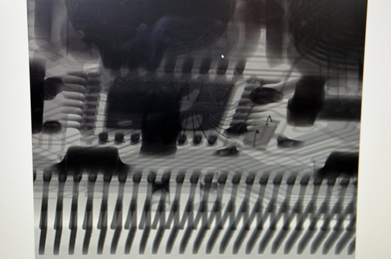
“In power electronics it is, for example, important that no bubbles, i.e. gas pockets are produced when soldering,” explains Professor Dr. Artem Ivanov from the priority research area of Electronics and System Integration. “With the help of the new x-ray system such defects inside a populated PCB can be easily identified.” Another possible use is for checking bonding wires, which are thinner than a human hair. Due to the high image resolution and magnification in the micrometre range, defects are also visible that otherwise would not be detected. In addition, it is possible to individually accentuate and view the copper layers that overlie one another in a PCB. “In this way the students become familiar with the latest standard technology using digital detectors,” smiles Ivanov, and adds, “They are guaranteed to find every defect with this.”
More equipment for materials analysis
The new x-ray microscope complements the existing high-quality laboratory equipment for materials research, which, among other things, also includes a high-resolution scanning electron microscope and a nanofocus computed tomography scanner. Whilst the scanning electron microscope is used to examine the surface structure of samples using an electron beam, the computed tomography system makes it possible to carry out non-destructive 3D defect analysis and quality assurance, by scanning components. These machines can also be used by companies for industrial applications.
Photo: Landshut University of Applied Sciences
(free to use if source cited)
Image1: Professor Dr. Artem Ivanov views the magnified x-ray images from Landshut University of Applied Sciences on his screen.
Image2: The digital detector of the new x-ray microscope is adjustable making it possible to obtain three-dimensional images.
Image3: The researchers can see the inside of the component on the x-ray image of the populated PCB.
